Understanding Band Coupling in Solid-State Devices
Written on
Chapter 1: Introduction to Solid-State Devices
Solid-state devices are integral components found in nearly all electronic equipment. Gaining a thorough understanding of these devices is essential for enhancing build quality and achieving greater efficiency. This insight led to the development of my algorithm, which utilizes the discontinuous Galerkin method for simulation.
Having successfully incorporated a spatially varying effective mass for electrons into my code, the next step involves addressing band coupling within the devices I am simulating. This topic will be the focus of today’s discussion.

Image by akitada31 on pixabay.
Chapter 2: What is Band Coupling?
Band coupling refers to the interaction that occurs between distinct energy bands within a solid. Electrons inhabit specific energy levels termed bands, each with unique energy gaps. When two bands are in close proximity in terms of energy, they may interact and overlap, leading to band coupling. To conceptualize this, consider the atomic lattice of the solid, which can be visualized as having 'lines' that correspond to similar energy levels. These lines construct energy bands throughout the three-dimensional structure, with alternating energy levels.
Section 2.1: Understanding Energy Bands
First, let’s clarify what is meant by a band. It is not a musical group; instead, it refers to the phenomenon where atoms bond and form molecules. The overlapping of atomic orbitals leads to the creation of bands. The outer shell of an atom is called the valence shell, which gives rise to the valence band. In contrast, the inner shell(s) contribute to the conduction band.
Bands are essentially ranges of energy levels available to electrons. These levels correspond to specific quantum states and are arranged in a continuous spectrum. Within a band, electrons can move freely, although they are restricted to specific energy levels.
Valence bands represent the highest energy levels that electrons can occupy without causing ionization, while conduction bands denote the lowest energy levels that allow for electrical conduction.
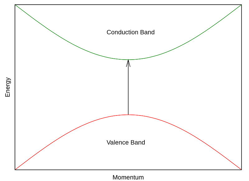
We can visualize these bands by plotting their energy levels against particle momentum:

The gap between the valence and conduction bands is referred to as the forbidden zone, or energy gap, which electrons cannot occupy. However, if this gap is sufficiently small and electrons possess ample energy (for example, at elevated temperatures), interactions may occur. This characteristic delineates conductors, semiconductors, and insulators. Insulators feature a larger energy gap, semiconductors have a smaller gap, while conductors, like copper, display no gap.
Section 2.2: Types of Band Coupling
There are three primary methods in which bands can interact with one another.
Direct Band Coupling
Direct band coupling involves the transfer of energy between different bands through direct electron-electron interactions. For instance, if electrons are present in the conduction band and holes (positively charged vacancies) exist in the valence band, electrons can transition between these bands. This process alters the energy of an electron without affecting its momentum.
In semiconductors, direct band coupling plays a crucial role in managing the movement of electrons and holes, thereby influencing the material's electrical characteristics. Moreover, it can also affect the optical properties of materials, such as light absorption and emission.
Several factors influence the strength of direct band coupling, including the density of states, the strength of electron-electron interactions, and the presence of impurities or defects.
Indirect Band Coupling
Indirect band coupling extends the concept of direct coupling. In this case, an electron's path to the conduction band is not linear but follows an oblique trajectory. This necessitates not only sufficient energy but also an impulse, typically provided by a phonon.
Various factors, such as the density of states, electron-phonon interaction strength, and the presence of defects, affect the strength of indirect band coupling as well.
Both direct and indirect coupling mechanisms are commonly referred to as interband coupling.
Intraband Coupling
Intraband coupling occurs when an electron vacates its position, creating a hole. Electrons within the same band can then move to occupy this hole. This process is essential for determining solid properties, as it impacts electrical and thermal conductivity, as well as optical and magnetic characteristics.
While typically weaker than interband coupling, intraband coupling can still significantly influence the properties of solids, particularly in materials with narrow energy bands.
Chapter 3: Practical Applications
The first video, "Fernco - Shear Banded Coupling Installation Video," provides insights into the installation process of shear band couplings, illustrating practical applications of coupling methods in engineering.
The second video, "Clamping Made Easy with BAND-IT Clamps - Gear Up With Gregg's," demonstrates the use of BAND-IT clamps, showcasing their effectiveness in various coupling applications.
Thank you for reading! If you found this information valuable, please consider giving a clap ?, and follow me on Medium and Twitter for more content. Interested in receiving my free weekly newsletter, "The Creative Engineer"? Subscribe here! For feedback, collaboration inquiries, or any questions, feel free to reach out via DM on Twitter or email me at [email protected]. If you'd like to support my work, consider buying me a coffee or donating via PayPal. Your support is greatly appreciated!